
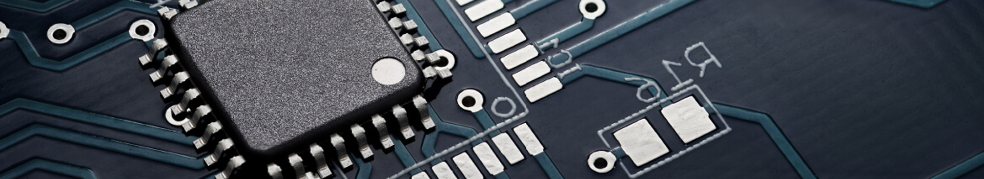
The challenges of package miniaturization
Packing more functionality into smaller devices brings many design, development, and volume manufacturing challenges. Creative package designs are all being put into play to achieve a smaller footprint, enhanced electrical performance, and thermal management while consuming less power.
Several critical challenges exist in implementing small packages. Die cracking and warping due to high stress are common failures. These conditions will worsen when using small and thin dies with a mismatch in the thermal expansion of the involved materials.
Small Pitch Design
Miniaturization goes along with pitch reduction. Decreasing the pitch size is critical in technologies used to achieve vertical interconnection in electronic packaging and integration. The hurdle to achieving this goal is getting the pins as close together as possible while surviving heat and maintaining connective stability.
For example, in buckling beam contacts, the maximum deflection will be design-dependent. As deflection increases, the radius of the buckle will get sharper until it reaches a critical value where the maximum fiber stress in the buckling beam exceeds the material yield stress. A buckling beam contact poses a problem regarding horizontal dimensions and thermal management that can reduce functionality while increasing failure risk. As the internal temperature rises, the connection weakens, losing its deflection force and connectivity.
With our patented H-Pin, a pure vertical pitch that can withstand temperature, providing current carrying capacity, and having very stable electrical characteristics is a real possibility. The pin motion moves perfectly up and down within the set confines of the outer dimensions, allowing for tighter design constraints and stable current, all without risking component failure.
Accelerated Testing
Most semiconductor devices have lifetimes that extend over many years of everyday use, but we cannot wait years to study a device. Applied stress tests enhance or accelerate potential failure mechanisms, help identify the root cause, and help semiconductor manufacturers prevent the failure mode.
In the production process, semiconductor devices may contain flaws due to the interference of tiny particles or differences in production equipment and the operation of reading semiconductor samples.
To reduce the failure rate, semiconductor producers seek to improve quality by introducing an assessment process that can include stress, burn-in, and other tests to meet reliability and certification requirements.
Our innovative automation, manufacturing, assembly, and connector assembly processes have empowered us to implement automated inspection and measurement into each manufacturing step. We have eyes looking at our intercomponents at the stamping, before assembly, and coming out of assembly going into the insertion machine. This fully-automated process control eliminates human error.
Combining Current Carrying and Stable Resistance and Electrical Performance
Over the past six decades, computers that once spanned the space of entire rooms have become miniaturized to fit in the palms of our hands. Even as traditional computing methods reach theoretical (and economic) chip and processor density limits, new high-performance computers, and even quantum computers continue to push boundaries.
It comes down to the size of internal components, component count, and their manufacturing process. Our extremely small, patented H-Pin, is produced through a cost-effective, fully-automated manufacturing process. It was custom-designed to increase performance, reduce costs, and provide trackable process controls.
The H-Pin: A Failproof Miniaturization Solution
From the accurate placement of the tiniest components to the necessity of designing customized hybrid and high-density components, the challenge is innovating while keeping test and manufacturability in mind. Plastronics works with some of the most innovative names in computing to find new ways to exceed the dimensional boundaries of semiconductor fabrication and packaging.
For spring-loaded probes pins, high-performance characteristics are defined by the ability to withstand high temperatures required for burn-in and other tests, the ability to handle increasing amounts of current over increasingly smaller pins, and the ability to handle high frequencies.
Too many design constraints compromise stable electrical performance and current carrying capacity with temperature and travel. Something will give. The only way to truly accommodate those design features is with the H-Pin. With the H-Pin and all its variations, you no longer have to choose between cost and performance. Now there's a high-performance, compliant contact made to serve high-volume applications requiring reliable electrical, mechanical, and thermal performance – all for a project-enabling cost.
We work with semiconductor test leaders using high-temperature operating life (HTOL) and highly accelerated stress testing (HAST) processes, which only strengthens the structure of our H-Pin manufacturing efforts. The tests provide an operational survivability test of computer chips, and board assemblies before leaving the manufacturing factory.
Our connectors are tested and proven to survive these extreme conditions before your electronics kit assembly.
Ready to talk through your application needs? Schedule a quick consultation. Nothing is too extreme for us. What you thought was small and fast can be smaller, faster, better.