
Semiconductor integrated circuits are critical elements in just about all electronic equipment, from microwave ovens to smartphones to supercomputers. Semiconductor sales in 2021 are expected to reach $500 billion, made possible by a highly complex manufacturing process that produces devices with both extreme complexity and extreme reliability. A current-generation microprocessor or graphic processor can contain over 50 billion transistors and exhibit a failure rate close to one per billion devices.
The role of testing
Testing during manufacturing plays a key role in ensuring reliable and repeatable performance. A semiconductor fabrication plant combines precise control of every process parameter with testing at each stage of production to weed out faulty parts as early as possible.
Semiconductor die are first tested for basic functionality at the wafer level. Any failures are discarded, and devices that pass are separated into individual units and placed into packages. Further testing awaits; before an integrated circuit leaves the factory, it will be tested as many as 20 times.
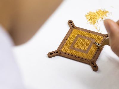
Most testing is performed by purpose-built equipment that connects to the chip, stimulates it with electrical signals to mimic real-world conditions, and captures the chip’s responses to see if they are correct. Known as automated testing equipment (ATE), these systems commonly sell for $1 or $2 million and can be programmed to test a variety of devices over many years. Figure 1 shows spring probes being loaded into an IC test socket that will be used with an ATE system to confirm the IC’s quality.
Figure 1. This image depicts a test socket being prepared for use on an ATE system.
Introduction to semiconductor test sockets
In order for the ATE to test the chip, there must be a physical connection with a clean electrical signal path established. A test socket is a custom-designed electro-mechanical interface that delivers extremely clean electrical signal paths to connect the chip to the ATE.
A typical test socket consists of three components:
- The socket body or cartridge is a customized piece of metal and plastic with precision cut cavities.
- Spring probes (or pins) are inserted into the hole cavities to provide an electrical path with mechanical compliance that will connect the chips to the test system.
- Depending on the application, the socket will have mechanical features such as a lid, retainer plate, or frame to create a robust mechanical interface.
Designers of test socket must deal with numerous challenges. The test socket must be extremely rigid and insensitive to changes in temperature and humidity for accurate and repeatable connections to the device being tested. The precise details depend on the type of device being tested, but probe pins must typically have low contact resistance; be able to carry high levels of current; and handle high-speed signals with multi-gigahertz data rates. The signal path must be shielded to minimize the effect of electromagnetic interference.
And, of course, the socket must operate successfully in a high-volume production environment, reliably handling millions of devices over many years. Consequently, electro-mechanical features must be simulated, modeled and designed to strike the optimum balance of signal fidelity, compression force, usability and durability to meet the production application.
Test sockets are custom designed to match the footprint and layout of a specific device, and are designed around the chip’s specific mechanical and electrical requirements. As data rates and bandwidth continue to increase, socket suppliers are performing more detailed electrical simulations during development. The analysis often includes the device package and PCB interfaces because of their impact on final socket performance in the system.
The dimensions and tolerances of the test socket body, as well as the spring pins that go into the socket body, are extremely small and extremely tight. Precision manufacturing and assembly is required to build a test socket, along with rigorous testing and simulation during the development process; as a result, the cost of a test socket can vary significantly.
Smiths Interconnect semiconductor test solutions
Smiths Interconnect provides high quality test sockets with a wide range of spring contacts and design standards; flexibility, design and fast delivery provide an optimal cost-to-performance ratio. Test sockets are available for a wide variety of leaded and leadless package types, including quad flat, no leads (QFN), quad flat pack (QFP), small outline integrated circuit (SOIC), ball grid array (BGA), land grid array (LGA) and more. Figure 2 shows test sockets for a variety of applications. Test socket categories include the following.
Figure 2. Test sockets for different applications.
Area array test
Test sockets in this category support testing of high pin count and high-speed signal products such as GPUs, CPUs and similar devices. The test socket design structure ensures low power inductance, high current carrying capacity and low contact resistance.
Peripheral package test
Peripheral ICs are widely found in wireless communications, automotive and industrial applications. The Joule-20 scrubbing contact technology provides first-class electrical and mechanical performance in testing peripheral ICs. The drop-in socket design allows the housing to be disassembled without removing the socket from the PCB. This enables cleaning and repair to be done without taking production equipment offline, reducing equipment down-time and improving production throughput. The Celsius series features continuous current capability up to 5 A and supports testing from -50° C to 170° C.
Package on package test
Package on package (PoP) devices are used in smartphone CPUs, digital cameras and wearables to provide maximum component density. The Euclid PoP Test Socket accurately and simultaneously aligns both the upper and lower device pads to increase fault coverage and reduce test cost. A customized socket design can test high speed signals in both system-level test (SLT) and ATE applications. Controlled impedance loop-back with PCB adds high-speed signal integrity.
Product spotlight: DaVinci test socket
Figure 3. DaVinci 56 test socket.
Consumer demands for next generation technologies such as 5G, AI, deep learning, vehicle-to-vehicle communication and self-driving vehicles fuel a need for high-speed data transfer and processing technologies. The DaVinci Series array test socket meets these requirements with an impedance-controlled coaxial solution at speeds up to 67 GHz analog RF and 112Gb/s digital.
Designed for high-speed testing of large IC packages, the DaVinci series utilizes spring probe technology in a patented insulated material housing, resulting in a coaxial structure with a reduced test height and low material deflection. DaVinci 56, the latest addition to the series, is a solution for 0.65 mm pitch and larger devices, for reliable testing up to 67 GHz analog RF and 112Gb/s digital.
Conclusion
Smiths Interconnect is a leading provider of technically differentiated electronic components, subsystems, microwave and RF products that connect, protect and control critical applications in the commercial aviation, defense, space, medical, rail, semiconductor test, wireless telecommunications and industrial markets. The company has 25 sales, R&D and manufacturing locations in 12 countries in the Americas, EMEA and Asia-Pacific.
The test socket is a key part of the semiconductor fabrication process, but designers must meet increasingly different challenges as package types proliferate, sizes shrink and speeds increase.
Smiths Interconnect‘s test sockets are optimized to provide superior quality and reliability to a variety of stringent semiconductor test applications. The company’s best-in-class engineering, development and technical expertise ensure support of automated, system level and development test platforms for area array, peripheral, wafer level and PoP devices.