

- Use of standard VME bus architecture cages for high speed fibre channel connection.
- Bandwidth: Up to 3 Gigahertz
- P1 and P3 Mounting dimensions
- Board to board high speed data transfer
- Matched Impedance Differential Pair Twinax & Quadrax
- Data sampling rates exceeding 2 Gbits/second
- 21 position true differential pair blind mate contacts
- 150 and 100 Ohm matched impedance
-
Rugged D-Sub with Twinax/Quadrax contacts
Split pair quadrax is the next generation contact that provides robust high-speed performance compatible with existing qualified rugged D-Sub connectors.
-
Fibre Channel D-Sub
Utilizing a multi-finger ground spring fixed around the shell to provide a multi-point contact engagement that affords superior EMI shielding.
-
Micro Quadrax/Twinax
Feature matched impedance miniaturized connectors that provide the user with controlled impedance and tightly spaced PCB footprint spacing.
-

Challenges Semiconductor Package Size and Pitch Face in Shrinking Consumer Electronics
Tiny computers, smartphones, and small electronic devices that industry leaders and other companies have popularized are forcing the hand of semiconductor package designers to shrink the package to fit within these little hand-held gadgets. The demand for technology applications, such as smart homes, smart manufacturing, smart medical care, and automotive electronics, continues to increase. At the same time, the requirements of continuous miniaturization and functional diversification of electronic product demands also increase.
-
?ext=.jpg&width=480&resizemode=force)
Raising the Bar of Burn-In Testing Sockets
Burn-in testing is widely used as an aid in producing failure-free electronic components. When scientifically planned and conducted, burn-in-testing sockets offer one of the most effective methods of reliability screening at the component level. Testing during production plays a vital role in ensuring reliability and repeatability. Semiconductor manufacturing plants perform tests at each stage of production to eliminate defective parts as early as possible while precisely controlling each process parameter of the chip.
-
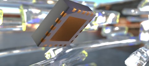
Optimizing Production Test of QFN-packaged IC’s for Consumer, Automotive, Industrial and Power Applications.
Where best-in-class electrical requirements intersect with a need for a small outline, low-profile footprint, IC designers are increasingly migrating to QFN packages. Meeting these testing challenges requires a test socket solution that is robust, reliable, and electrically “clean.”
-
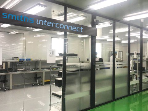
Test Laboratory Expansion in Suzhou
The Centre of Excellence will offer a one-stop-shop to the global customer base for the products used in semiconductor test applications.