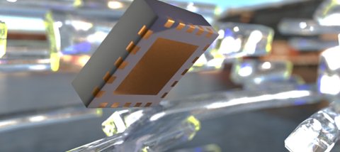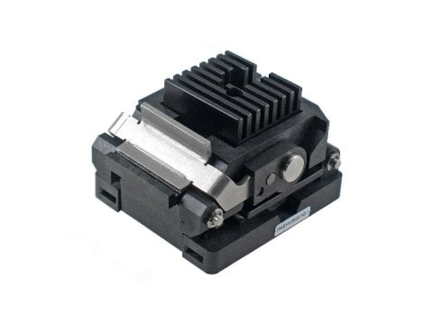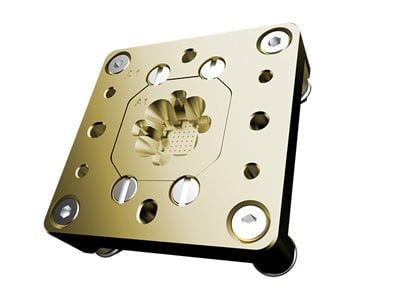
Technical Features:
- For testing LGA, QFN, QFP and other variants
- Scrub action breaks through surface oxides on device pad
- Short signal path
- Tri-Temp socket design to support -55 °C to +150 °C
- Configurable design flexibility for integrating into existing hardware setups
- Designed for manual test, bench test, and HVM production test
- Insulator housing made from high-performance polyimide
- Small socket footprint
Benefits:
- Long contact life, low wear, tested to over 500K insertions
- Provides reliable and consistent contact for Matte Tin or NiPdAu pads, low consistent Cres
- Exceptional signal integrity
- Covers wide range of test applications
- Match existing PCB socket footprint and test hardware lead to cost saving for customers
- Field repairable, easy cleaning and maintenance
- Low Dielectric constant, Low CLTE, exceptional Flexural Modulus
- Allows for PCB topside components to be placed close to DUT for better signal performance and less signal loss