
The process of innovation and semiconductor testing takes time and money, so how do you make testing and manufacturing processes more affordable and efficient? Let’s talk more about optimizing space on circuit boards and how this can be a domino effect for time- and cost-efficiency.
Optimizing socket use in burn-in testing
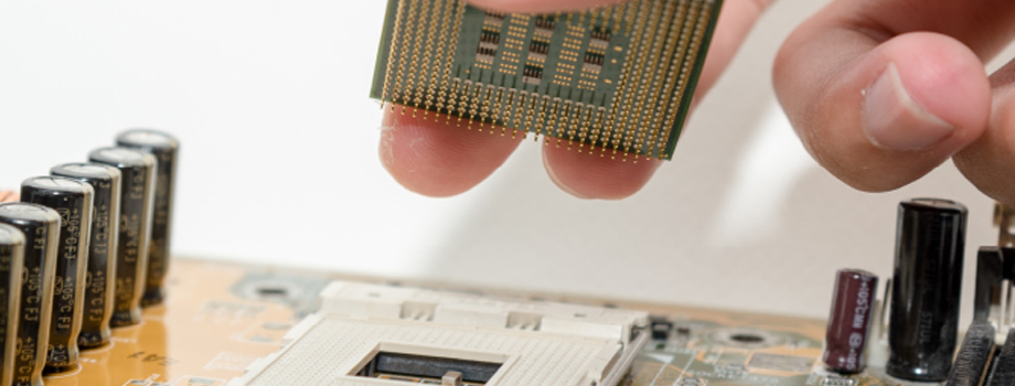
Burn-in is a testing process designed to detect early life failures in semiconductor devices and reduce the potential for defects and catastrophes in the field. During burn-in, semiconductor devices endure extreme operating conditions, including elevated temperatures, high use cycles, and high voltages. The goal is to eliminate defective parts or those with short lifespans before they can become a factor in a system failure.
Reliability burn-in requires a few necessary items: a burn-in board, sockets, and a system to provide the signal, power, and temperature regulation needed to stress the device under test (DUT).
Reliability Burn-In Standards are set by the JEDEC Solid State Technology Association and require a specific number of sockets. For example, let’s say you have to buy multiples of 80 – for reliability burn-in testing. If you have to buy 80 sockets at $100 per socket, and spread those sockets out across two to four circuit boards, that’s quite a bit of space and money being spent.
That’s where multisite sockets come in. Wouldn’t it be great to have a socket which could house more than one device?
Instead of buying 80 sockets, you could decrease the number of sockets and increase the number of rest positions. Not only is it then possible to decrease the number of burn-in boards, but it frees up capacity in the burn-in chamber. It is much more efficient to load a socket with 2-4 positions versus loading one socket at a time, so it is an added benefit that labor costs are potentially reduced.
Multisite doesn’t mean compromising on signal
But do more packages on a single socket mean you’re losing signal or performance? Not at all.
With our sockets here in the Smiths Interconnect Semi Test Business Unit, we do not compromise on raw materials, components, or manufacturing processes.
For example, we still use the H-Pin to provide a high-performance socket that is affordable for all burn-in operations. The H-Pin is a stamped spring probe with the mechanical, electrical, and thermal performance of a spring probe and the ease of use and high volume manufacturability of a stamped contact. It serves applications without the typical compromises required when considering cost versus performance.
Download the H-Pin Guide
Why we use the H-Pin:
- Improved electrical performance: Designed to provide excellent electrical and mechanical performance, H-Pins reduce the risk of damage to the electronic component during insertion and removal. They provide a calculated contact force, which ensures a secure and stable connection between the component and the socket or connector. The H-Pin design also reduces contact resistance, leading to better electrical performance.
- Better signal integrity: H-Pins provide a more constant and consistent contact force across all the pins, ensuring the signals transmit uniformly without loss or distortion. This leads to better signal integrity, improved data transfer rates, and reduced noise.
- Enhanced durability: Made from BeCu with a stainless steel coil spring that can withstand high temperatures and mechanical stress, H-Pins are more durable than other contact pins with a longer life span, leading to lower maintenance costs and reduced downtime.
- Compatibility: H-Pins can be used in a wide range of electronic applications, making them a versatile solution for electronic sockets, connectors, and adapters.
How do you know when multisite sockets are right for your burn-in testing?
Having been in this business for over 50 years, and having built the strong relationships we have with our customers and partners, we are able to truly understand and predict the situations that call for multisite socket use.
Ultimately, we know that many of our customers are facing pressure to “do more with less”, which is why we will make sure they know when to utilize multisite sockets.
There are some complex cases when multisite sockets aren’t the right choice – most have to do with minimizing the proximity of high voltage and high-temperature components. Having these interconnects too close together may affect each other thermally, mechanically, or electrically. This would be the primary case in which multisite sockets would not be ideal.
Other ways we make testing and manufacturing more affordable and time-efficient
Whether your challenge is cost, capability, lead time or quality, we have the in-house technologies and manufacturing capabilities to solve your burn-in and test challenges. From decades of experience and flexible tooling, to standard product lines and the world’s greatest pin technologies, our customers are saving money and shipping quality parts out the door.
Our patented technologies are based on solving the difficult industry problems associated with high frequency, high current, low resistance and adequate contact travel. Furthermore, our unique automated manufacturing process ensures that you get the quickest lead-times on any new project or modifications to existing products.
In addition, we are a U.S.-based socket supplier with a global footprint that enables us to offer unprecedented flexibility and responsiveness for semiconductor companies, circuit board manufacturers, and burn-in service providers across the world.
Benefits of our test sockets
We’ve been raising the bar of burn-in testing sockets for years. Our socket solutions offer several advantages over traditional socket solutions, including:
- Higher pin counts: Our sockets can accommodate higher pin counts, making them suitable for high-performance electronic devices.
- Greater design flexibility: We offer greater design flexibility, allowing for customization and optimization of the socket design to meet specific application requirements.
- Reduced manufacturing time: Sockets are produced through automated assembly, reducing manufacturing time and costs.
- Improved electrical performance: We provide socket solutions that offer enhanced electrical performance, with better signal integrity, lower crosstalk, and better impedance control.
Quick recap: top 3 benefits of multisite burn-in test sockets
-
Save money on purchasing fewer sockets
-
Save space by using one socket in multiple positions
-
Save time on labor and manufacturing