
The telecommunications industry and community have been dealing with the issue of radio spectrum allocation and congestion for many years. Radio spectrum represents a natural resource whose allocation must be carefully managed to achieve its optimal use. Over the last few decades, standard 2.4 GHz band radio spectrums have become more congested and demand for prime positioning in this radio band spectrum is limited.
The most natural way to reduce the problem is by allocating higher frequencies to new applications. This shift of radio wave ecosystems towards higher frequencies brings its own challenges, as RF chip components are getting increasingly smaller and more complex to manufacture.
To properly support introduction of new technologies at high frequencies, all aspects of component design and development must be considered including the choice of high frequency fixture, test board preparation, proper DUT installation and finally, production-level testing. New design techniques must be applied through RF simulation tools, improved controlled manufacturing processes and utilizing more accurate test fixtures and procedures.
Test Board Preparation:
During preparation carefully inspect all the components of the test fixture to be assembled (test boards and DUT chips) for any damage and burrs. Rough edges of the test board may cause fixture assembly issues and therefore should be cleaned up using fine grit sandpaper.
*Important to sand square and evenly and always finish with a very fine grit (600 min.)
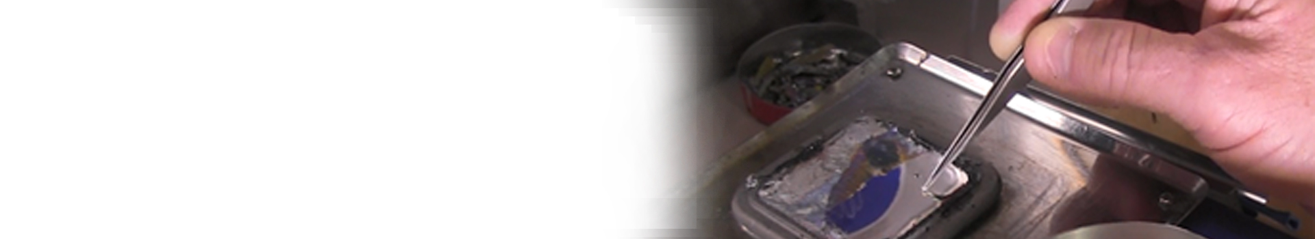
Proper Installation (SMT and Wire Bonding):
SMT, Surface Mount Installation:
For proper SMT installation chip terminations need to be properly centered and aligned. Surface mount installation (SMT) usually consists of chip (DUT) tinning, flux application to the test board, chip positioning (placement) and reflow.
Wire Bonding Installation:
Wire bonding is generally considered the most cost-effective and flexible interconnect technology and is used to assemble the vast majority of semiconductor packages. For proper wire bonding installation pay close attention to the cleanliness of the parts and equipment, preheat the parts to be bonded (adjust the temperature based on the bond metallization as well as the type and size of wire or ribbon)
*Short ribbon bonds with the width equal to that of 50 ohm transmission line provide the best RF performance.
Mounting:
The final step in the fixture assembly is mounting the connector on the test board. Then, the DUT is to be installed which starts with the careful inspection of all the components of the test fixture to be assembled. Special attention should be given to the test board edges as common PCB manufacturing often leave rough edges that can cause fixture assembly issues. The edges of the test board can usually be cleaned up using fine grit sandpaper. The DUT tends to move during solder reflow. To prevent this, pure indium solder could be used. The indium solder is very soft and the DUT can be pressed into the solder before reflow which allows for fine adjustment of the DUT to the transmission line and insures that the DUT is flush with the test board. When the DUT is reflowed, it remains in place. Finally, the DUT need to be connected to the transmission line. The standard practice is to center the connector pin on the transmission line and ensure that the connector is flush with the edge of the test board to avoid any undesired air gaps. There are primarily two types of connection methods - ribbon and wire bonding. Short ribbon bonds provide the best RF performance, but wire bonding is the most popular.
*Always follow best practices in connector installation that are usually supplied by the connector.
Production-level (high-volume) Testing:
In production-level RF test, DUTs must be verified for RF performance by test methods that use non-solder contact of signal and ground pads. This test method is referred to as ‘push-on’ testing. The development of a push-on test fixture in addition to the design of an RF component is an essential part of each project. This approach results in an establishment of a good correlation between soldered and non-soldered performance of the tested RF component as the PCB is the same structure in both measurements. Having a push-on fixture enables a non-destructive test that is required in many applications. The non-destructive test fixture may be fully developed and tailored to a specific design or a standardized pre-manufactured test fixture used.
For additional support on fxiture preparation and RF test please download our White Paper: Fixture Preparation and RF Test of SMT Board Level components at High Frequencies.
The development of RF components that operate at increasingly higher frequencies requires new simulation techniques and test methodologies that consider the specific behavior of electromagnetic waves at frequencies of Ka-band and above. The test fixture in a sense electrically becomes the part of the DUT that affects its performance. This poses a significant challenge as the electrical performance of an RF device can be guaranteed only in a specific environment. Through collaboration between the RF component development team and the customer, all the necessary information about the application of the to-be-developed RF component is to be used to optimize the RF component for the best possible performance.