

To keep up with the dramatic progress in mobile phone development, chip suppliers must bring up new silicon quickly, predictably, and at the lowest costs possible. A variety of test setup challenges must be overcome in order to ramp a WLCSP device into high volume on schedule. The probe head required to connect a WCLSP device to the ATE can be a critical link. Any delays caused by readiness of the probe head to support characterization, debug, or production release of the chip and its test program can be disastrous for a supplier in this space.
Manufacturers must select a vendor and a probe head architecture that deliver maximum return on investment – both in the engineering lab, and on the HVM production test floor. The ideal setup will allow flexibility for the test engineer to change between multiple environments, from single-site to multi-site, from singulated die to full wafer test, and from characterization / debug to production test. The re-use of test hardware across these varied applications can provide substantial cost savings, as the efforts in these spaces are typically sequential.
The single most important aspect in developing a probe head for a WLCSP application is ensuring that hardware is ready on time, every time. Once the package dimensions are known, and a multi-site wafer probing pattern is decided, the test engineering team must work quickly to get a probe head designed, manufactured, and delivered on time, in order to properly support the bring up efforts. By standardizing design elements and designing for HVM multi-site up front, a single probe head design can be produced that addresses all the chip supplier’s requirements.
A particular challenge in WLCSP test engineering teams is being ready to support either singulated-die setup or complete wafer setup. In many cases, an MPW (Multi-Product Wafer) will be procured from the wafer fab, resulting in singulated bare die being the first units to arrive at the lab floor. In order to test these units, the test engineer must have a probe head that can be quickly configured to test one or multiple die in a manual hand-test setup. A lid solution must be available to compress the die onto the probe head, and the electrical performance of the setup must be nearly identical to the full wafer setup.
When full wafers are available, test engineering teams must move quickly to validate multi-site test programs, considering the potential for site-to-site variation across a large array and the associated electrical fan out. All the mechanical and electrical considerations of the multi-site stack-up, from the ATE pogo pin to the wafer, must be carefully planned for in advance to keep HVM production release on schedule. Any mis-match between initial bring-up done on singulated die or a partial wafer can cause painful delays. For the most fine-pitch applications (below 250µm) the interface stack up will often necessitate the added challenge of a fan-out or “space transformation” solution to adapt the WCSLP pitch to the PCB pad pitch. The ability to debug each site’s signal path across a multi-site array prior to arrival of the full wafer can reduce risk substantially.
Once the multi-site probe head is released to production, it must provide reliable, robust performance in a harsh, high-volume environment. The probe head should be easy to clean, easy to repair, and deliver hundreds of thousands of insertions with stable yields. When a probe head needs to be serviced, it must be returned to production quickly, with minimal effort required by the OSAT partner to replace or repair individual probe elements.
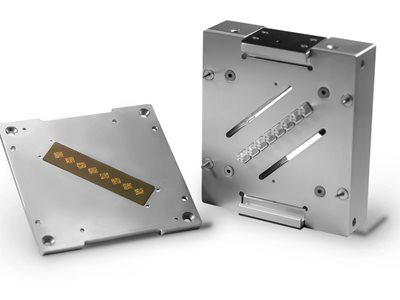
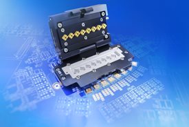
The Volta Series Probe Head addresses a need for reduced test time set-up and increased throughput in high reliability testing of Wafer Level Packages (WLP), Wafer Level Chip Scale Packages (WLCSP) and Known Good Die (KGD) at 180 µm pitch and higher.
The Smiths Interconnect’s “Volta” line of WLCSP probe heads meet these challenges, with options ranging from 500µm to 180µm pitch for a full grid array. For device pitches below 250µm, the Volta Fan-Out PCB can be used to route the probe head onto a standard 400µm or 800µm pitch PCB. It’s design process is robust and predictable, thanks to Smiths Interconnect’s extensive experience working with many of the industry’s leading WCLSP chip suppliers. Within weeks, a single probe head design is produced that can accommodate singulated die testing, single-site to 128-site bring up, and reliable HVM production. The Volta architecture merges best in class spring probe technology with an industry-leading coated metal housing. The result is a probe head that can be delivered quickly for bring-up and re-used for over 1M touchdowns on an OSAT’s wafer sort production floor. Backed by Smiths Interconnect’s strong global presence, Volta solves your most demanding WLCSP bring up challenges with solid Total Cost of Ownership and ROI.